
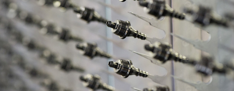
Offsite Plating Services: Precision Surface Finishing, Delivered Seamlessly
Managing complex chemical plating processes in-house can strain your facility’s footprint, resources, and environmental compliance. Our Offsite Plating Services provide a turnkey, outsourced solution for your high-reliability components. By leveraging our state-of-the-art automated plating lines, strict statistical process controls, and specialized engineering team, you get pristine surface finishes without the overhead of maintaining an internal plating line. Whether you need high-density leadframes, connectors, or intricate semiconductor substrates plated, we deliver rapid turnaround times and uncompromised quality directly to your production line.
Process Capabilities
Advanced, high-purity metallization engineered to tight structural tolerances.
| Plating Capability | Technical Specifications & Execution |
|---|---|
| Selective & Immersion Plating | High-speed, fully automated lines optimized for continuous strip leadframes and connectors. This ensures precise target deposit placement while drastically reducing precious metal waste. |
| Multi-Material Chemistry Portfolio |
We support versatile layer stackups tailored to your functional needs:
|
| Ultra-Thin Layer Control | Advanced bath dynamics allow us to safely deposit highly uniform, ultra-thin functional metallic layers down to sub-micron tolerances, maintaining strict component design clearances. |
| Custom Masking & Tooling | In-house tooling engineers design and manufacture custom masking fixtures to handle complex geometries, single-sided requirements, or proprietary selective plating schemes. |
Key Features & Advantages
Why Tier-1 semiconductor and electronics manufacturers choose our offsite finishing facility.
Advanced Metrology Lab
Every production batch is backed by rigorous quality validation, utilizing X-ray Fluorescence (XRF) for precise thickness verification, automated optical inspection (AOI), and tape-and-reel bake testing for adhesion.
Zero Footprint & Compliance
Transitioning your plating offsite completely eliminates the operational burden of toxic chemical waste management, environmental permitting, and maintaining expensive scrubbing systems at your facility.
High-Volume Scalability
Powered by fully automated inline chemical bath monitoring and real-time replenishment systems, we guarantee perfectly consistent layer morphology from initial prototype validation up to multi-million unit production runs.
Turnkey Logistics
Optimized supply chain pipelines featuring specialized climate-controlled packaging protocols and dedicated logistics to ensure your highly sensitive components are plated, verified, and returned on time.
Our Semiconductor and PCB Films
Various Application and Customizations

Singulation Tape
Secures Chips During cutting; Offers precise UV release.

Backgrinding Film
Supports wafers during thinning; prevents breakage.

Heat Release Film
Supports package dicing; prevents breakage and residue Free.

Toyo Adtec Precision Pre-Cut Dicing Films: Streamline Your Singulation Process
Zero Airborne Contam and Perfect Frame Alignment Fit to customer needs.

Backgrind Tapes
Supports wafers during thinning; prevents breakage.
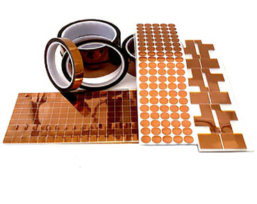
Polyimide Film
Paired with high-performance silicone or acrylic adhesives, it peels away perfectly clean after processing, leaving zero residue on precious gold contacts ("gold fingers").