
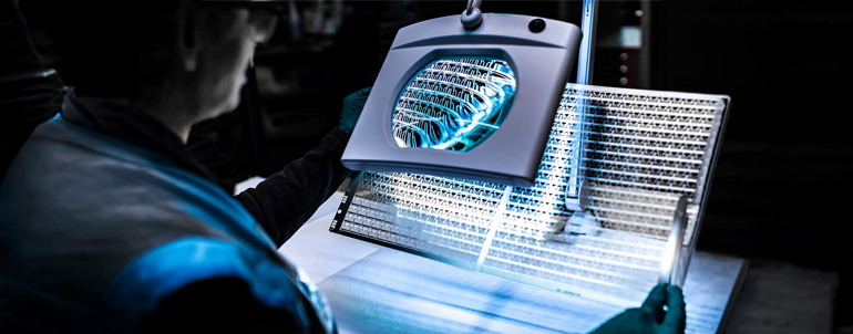
Toyo Adtec Leadframes powered by Ningbo Gangbo Electronics Co., Ltd.
Established in 1991, Ningbo Gangbo Electronics is a premier precision manufacturer specializing in critical backend semiconductor integration components, high-density manufacturing matrices, and deep chemical subtractive technologies.
Core Product Portfolio
Integrated Circuit (IC) Lead Frames
High-density structural configurations tailored to secure silicon dies and deliver pristine connection profiles across standard multi-pin package arrays like Small Outline Packages (SOP) and Dual In-line Packages (DIP).
Discrete Device Frames
Specially stabilized copper architectures manufactured to match exact mechanical footprints for foundational discrete components including transistors, small-signal diodes, and standard SOT surface-mount form factors.
Power Series Lead Frames
Heavy-duty layouts structurally optimized with thick copper frames and maximized thermal conductive paths to support high-voltage power modules like MOSFETs, IGBTs, and thyristors.
Etched Ultra-Fine Pitch Series
Engineered via chemical subtraction processes instead of mechanical punches, allowing ultra-thin profiles, matrix layouts, and tight pad margins required for high-density QFN/DFN chip architectures.
Advanced Manufacturing Capabilities
In-House Progressive Die Fabrication
Independent construction and maintenance of high-precision dynamic progressive stamping tools, giving electronics manufacturers rapid customization channels and custom design adaptability.
Automated Multi-Station Stamping
High-speed manufacturing facilities fitted with specialized high-tonnage automated pressing units, ensuring low defect rates across massive corporate supply allocations.
Precision Chemical Etching Lines
Advanced chemical-mill pathways that safely render micrometer-level trace definitions without introducing stamp shear stresses onto delicate raw copper strips.
Selective Surface Electroplating
Highly targeted continuous functional plating capabilities (such as localized silver zone plating) to secure robust wire-bond interfaces and avoid packaging oxidization paths.
Copper Leadframes Product Line
Etch and Stamp Integration Systems
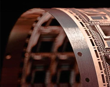
Etch Leadframe
High Density DFN/QFN Substrate Architecture Support.
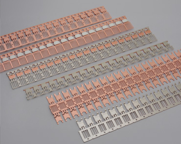
Legacy Products
Power Management ICs, Analog ICs, MCUs, Sensors, MEMS, and Discrete Semiconductors.
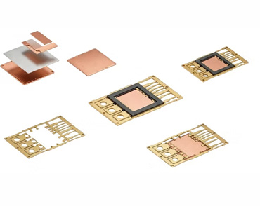
Bridge Leadframes
Multi-Die Accommodation, Heavy-Gauge Copper Metals, and Massive Thermal Mass Capabilities.
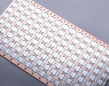
LED IC Leadframes
SMD, Through-Hole, and High-Power LED packaging applications with optimized lumen stability.
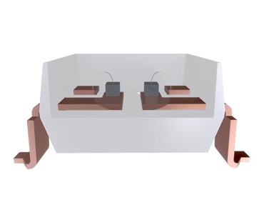
OptoCoupler & PV Leadframe
Premium Optocoupler and Photovoltaic IC Leadframes built for harsh industrial signal isolation environments.